> ## Documentation Index
> Fetch the complete documentation index at: https://mintlify.com/tiny-tpu-v2/tiny-tpu/llms.txt
> Use this file to discover all available pages before exploring further.
# Architecture overview
> High-level overview of the Tiny TPU hardware architecture
Tiny TPU is a minimal tensor processing unit reinvented from Google's TPU V1 and V2 designs. The architecture implements a complete hardware accelerator capable of executing forward and backward propagation for neural network training.
## System architecture
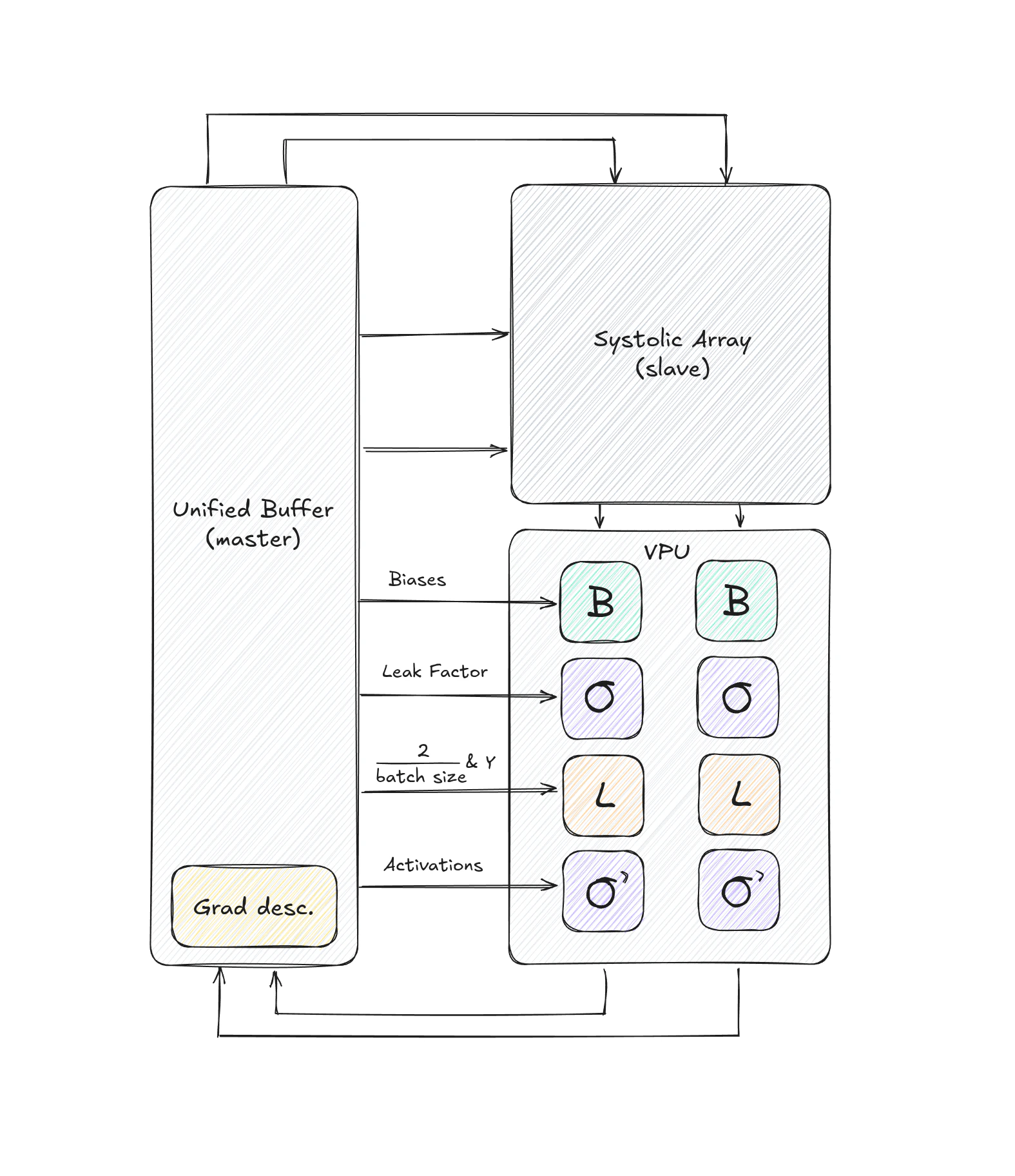 The Tiny TPU consists of five major components that work together to accelerate matrix operations and neural network computations:
1. **Processing element (PE)** - The fundamental computational unit
2. **Systolic array** - A 2D grid of processing elements
3. **Vector processing unit (VPU)** - Element-wise operations pipeline
4. **Unified buffer (UB)** - Dual-port memory for intermediate values
5. **Control unit** - Instruction decoder and system controller
## Top-level module
The top-level TPU module connects all major components:
```systemverilog theme={null}
module tpu #(
parameter int SYSTOLIC_ARRAY_WIDTH = 2
)(
input logic clk,
input logic rst,
// Write ports from host to unified buffer
input logic [15:0] ub_wr_host_data_in [0:SYSTOLIC_ARRAY_WIDTH-1],
input logic ub_wr_host_valid_in [0:SYSTOLIC_ARRAY_WIDTH-1],
// Read instruction inputs
input logic ub_rd_start_in,
input logic ub_rd_transpose,
input logic [8:0] ub_ptr_select,
input logic [15:0] ub_rd_addr_in,
input logic [15:0] ub_rd_row_size,
input logic [15:0] ub_rd_col_size,
// Learning rate and VPU control
input logic [15:0] learning_rate_in,
input logic [3:0] vpu_data_pathway,
input logic sys_switch_in,
input logic [15:0] vpu_leak_factor_in,
input logic [15:0] inv_batch_size_times_two_in
);
```
Source: [tpu.sv:4-31](https://github.com/tiny-tpu-v2/tiny-tpu/blob/main/src/tpu.sv#L4-L31)
## Data flow
The TPU follows a specific data flow pattern:
### Forward pass
1. **Input loading**: Matrices are loaded from the host into the unified buffer
2. **Systolic computation**: Input and weight matrices flow through the systolic array
* Inputs flow horizontally (left to right)
* Weights flow vertically (top to bottom)
* Partial sums accumulate vertically
3. **VPU processing**: Results pass through the VPU pipeline:
* Bias addition
* Leaky ReLU activation
4. **Result storage**: Outputs are written back to the unified buffer
### Backward pass
1. **Loss computation**: VPU computes loss derivatives
2. **Gradient computation**: Systolic array computes weight and activation gradients
3. **Activation derivative**: VPU applies activation function derivatives
4. **Parameter update**: Gradient descent modules update weights and biases
## Key features
### Fixed-point arithmetic
All computations use 16-bit fixed-point representation (Q8.8 format):
* 8 bits for integer part
* 8 bits for fractional part
* Signed values using two's complement
The fixed-point library in `fixedpoint.sv` provides modules for multiplication (`fxp_mul`), addition (`fxp_add`), and other arithmetic operations with overflow detection.
### Pipelined architecture
The VPU implements a pipelined architecture where multiple modules can process different data simultaneously:
```systemverilog theme={null}
vpu_data_pathway[3:0]:
0000: No modules active
1100: Forward pass (bias → leaky relu)
1111: Transition (bias → leaky relu → loss → leaky relu derivative)
0001: Backward pass (leaky relu derivative only)
```
Source: [vpu.sv:10-17](https://github.com/tiny-tpu-v2/tiny-tpu/blob/main/src/vpu.sv#L10-L17)
### Configurable dimensions
The systolic array width is configurable via the `SYSTOLIC_ARRAY_WIDTH` parameter:
* Default: 2×2 array
* Scalable to larger dimensions (e.g., 256×256, 512×512)
Larger array dimensions require modifications to the unified buffer size and interconnect logic.
## Performance characteristics
### Throughput
Each processing element performs one multiply-accumulate (MAC) operation per clock cycle:
* 2×2 array: 4 MACs per cycle
* Single-cycle operation for activated PEs
### Memory bandwidth
The unified buffer provides:
* Dual-port read/write capability
* Staggered data delivery for systolic flow
* Transpose support for efficient matrix operations
## Implementation details
### Clock and reset
All modules use synchronous design:
* Positive edge-triggered flip-flops
* Asynchronous active-high reset
### Data widths
Standardized 16-bit data paths throughout:
* Input activations: 16 bits signed
* Weights: 16 bits signed
* Partial sums: 16 bits signed
* Bias values: 16 bits signed
## Next steps
Explore each component in detail:
Learn about the PE multiply-accumulate unit
Understand the 2D PE grid architecture
Explore the VPU pipeline stages
Discover the memory architecture
The Tiny TPU consists of five major components that work together to accelerate matrix operations and neural network computations:
1. **Processing element (PE)** - The fundamental computational unit
2. **Systolic array** - A 2D grid of processing elements
3. **Vector processing unit (VPU)** - Element-wise operations pipeline
4. **Unified buffer (UB)** - Dual-port memory for intermediate values
5. **Control unit** - Instruction decoder and system controller
## Top-level module
The top-level TPU module connects all major components:
```systemverilog theme={null}
module tpu #(
parameter int SYSTOLIC_ARRAY_WIDTH = 2
)(
input logic clk,
input logic rst,
// Write ports from host to unified buffer
input logic [15:0] ub_wr_host_data_in [0:SYSTOLIC_ARRAY_WIDTH-1],
input logic ub_wr_host_valid_in [0:SYSTOLIC_ARRAY_WIDTH-1],
// Read instruction inputs
input logic ub_rd_start_in,
input logic ub_rd_transpose,
input logic [8:0] ub_ptr_select,
input logic [15:0] ub_rd_addr_in,
input logic [15:0] ub_rd_row_size,
input logic [15:0] ub_rd_col_size,
// Learning rate and VPU control
input logic [15:0] learning_rate_in,
input logic [3:0] vpu_data_pathway,
input logic sys_switch_in,
input logic [15:0] vpu_leak_factor_in,
input logic [15:0] inv_batch_size_times_two_in
);
```
Source: [tpu.sv:4-31](https://github.com/tiny-tpu-v2/tiny-tpu/blob/main/src/tpu.sv#L4-L31)
## Data flow
The TPU follows a specific data flow pattern:
### Forward pass
1. **Input loading**: Matrices are loaded from the host into the unified buffer
2. **Systolic computation**: Input and weight matrices flow through the systolic array
* Inputs flow horizontally (left to right)
* Weights flow vertically (top to bottom)
* Partial sums accumulate vertically
3. **VPU processing**: Results pass through the VPU pipeline:
* Bias addition
* Leaky ReLU activation
4. **Result storage**: Outputs are written back to the unified buffer
### Backward pass
1. **Loss computation**: VPU computes loss derivatives
2. **Gradient computation**: Systolic array computes weight and activation gradients
3. **Activation derivative**: VPU applies activation function derivatives
4. **Parameter update**: Gradient descent modules update weights and biases
## Key features
### Fixed-point arithmetic
All computations use 16-bit fixed-point representation (Q8.8 format):
* 8 bits for integer part
* 8 bits for fractional part
* Signed values using two's complement
The fixed-point library in `fixedpoint.sv` provides modules for multiplication (`fxp_mul`), addition (`fxp_add`), and other arithmetic operations with overflow detection.
### Pipelined architecture
The VPU implements a pipelined architecture where multiple modules can process different data simultaneously:
```systemverilog theme={null}
vpu_data_pathway[3:0]:
0000: No modules active
1100: Forward pass (bias → leaky relu)
1111: Transition (bias → leaky relu → loss → leaky relu derivative)
0001: Backward pass (leaky relu derivative only)
```
Source: [vpu.sv:10-17](https://github.com/tiny-tpu-v2/tiny-tpu/blob/main/src/vpu.sv#L10-L17)
### Configurable dimensions
The systolic array width is configurable via the `SYSTOLIC_ARRAY_WIDTH` parameter:
* Default: 2×2 array
* Scalable to larger dimensions (e.g., 256×256, 512×512)
Larger array dimensions require modifications to the unified buffer size and interconnect logic.
## Performance characteristics
### Throughput
Each processing element performs one multiply-accumulate (MAC) operation per clock cycle:
* 2×2 array: 4 MACs per cycle
* Single-cycle operation for activated PEs
### Memory bandwidth
The unified buffer provides:
* Dual-port read/write capability
* Staggered data delivery for systolic flow
* Transpose support for efficient matrix operations
## Implementation details
### Clock and reset
All modules use synchronous design:
* Positive edge-triggered flip-flops
* Asynchronous active-high reset
### Data widths
Standardized 16-bit data paths throughout:
* Input activations: 16 bits signed
* Weights: 16 bits signed
* Partial sums: 16 bits signed
* Bias values: 16 bits signed
## Next steps
Explore each component in detail:
Learn about the PE multiply-accumulate unit
Understand the 2D PE grid architecture
Explore the VPU pipeline stages
Discover the memory architecture